How do I describe surface roughness?
Roughness can be taken into account in different ways in optical models for thin films.
The easiest way is to replace the sharp interface between two materials by a thin layer with mixed optical constants. This is a good approach for roughness dimensions clearly below the light wavelength. Mixed optical constants can be computed using an effective medium model. The Bruggeman formula (also known as EMA – effective medium approximation) is a good choice (please read the remarks below). Start with a very thin intermediate layer (e.g. 2 nm) and select its thickness as fit parameter. The volume fraction of the effective medium model should be an adjustable fit parameter as well.
An advanced version of this kind of roughness modeling is to use a concentration gradient layer. This type of layer can describe a smooth transition between adjacent materials. The depth dependence of the volume fraction can be expressed by a user-defined formula with up to 6 parameters that can be fitted.
A warning must be raised using effective medium models to describe roughness effects. All effective medim models in our software are made for two phase composites which are isotropic in three dimensions. They are not valid for surface roughness effects. To apply these concepts anyway can be justified by saying that there is no reasonable alternative and that it is very common to do so …
Describing rough metal surfaces with an effective medium model may be a little tricky. This is especially true for silver. Inhomogeneous metal layers can be efficient absorbers with very special optical properties, and effective medium approaches can be very wrong – please read SCOUT tutorial 2 about this.
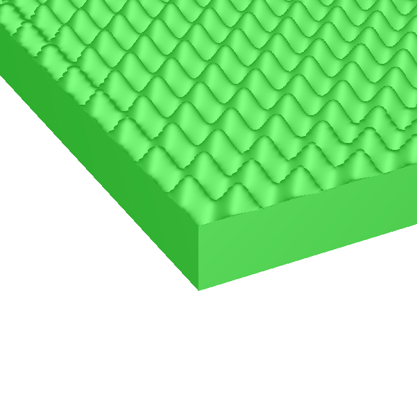
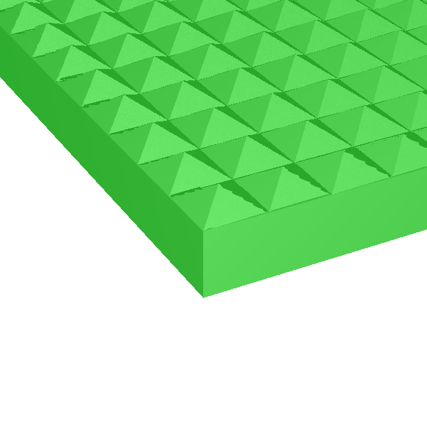
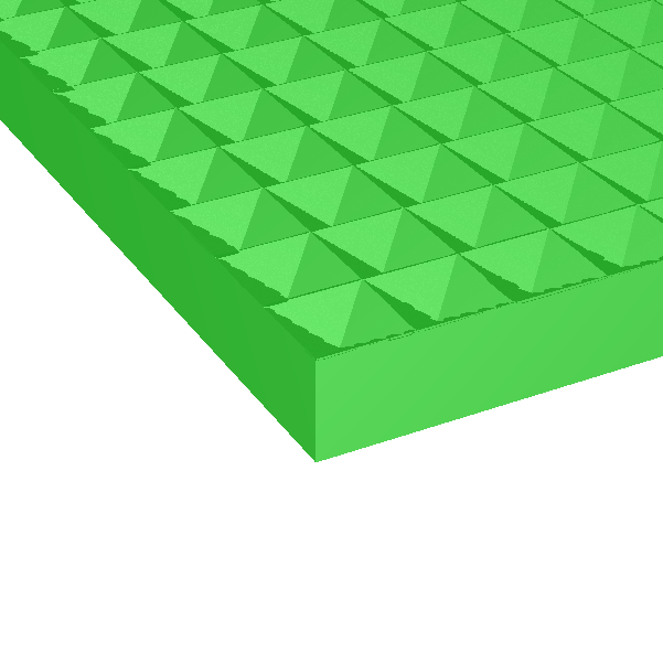
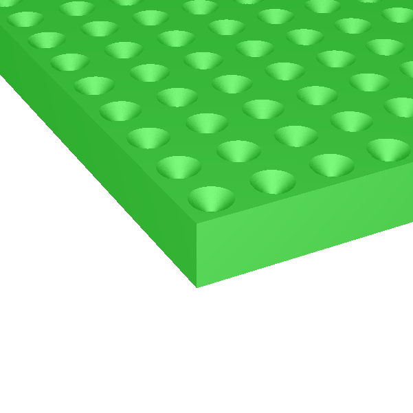
The roughness described by effective medium layers does not lead to light scattering but modifies the reflectance and transmittance properties of the interface between the adjacent materials. Light scattering at heavily rough interfaces can be taken into account in a phenomenological way in cases where the detection mechanism of the spectrometer system does not collect all the scattered radiation. You can introduce a layer of type ‘Rough interface’ which scales down the reflection and transmission coefficients for the electric field amplitude of the light wave. The loss function is a user- defined function which may contain 2 parameters C1 and C2 which are fit parameters. In addition, the symbol x in the formula represents the wavenumber.
The expression C1*EXP(-(X/C2)^2), for example, would describe an overall loss by a factor C1 and an additional frequency dependent loss which is large for small wavelengths and small for large wavelengths. This kind of approach has turned out to be satisfying in several cases.