After some problems with corrupted configuration files we have decided to update the workbook component, starting with object generation 5.28. We hope that all workbook function work as before. If you find issues please be patient and report to us what you found. We will then try to help you as quick as we can.
Category Archives: SPRAY
What makes the difference between a good and a very good optical model?
Answering some recent questions about optical modelling, I dug out some old slides. They explain some model improvements that were implemented a long time ago. Combined with today’s fast computer hardware they provide the basis of high quality modelling.
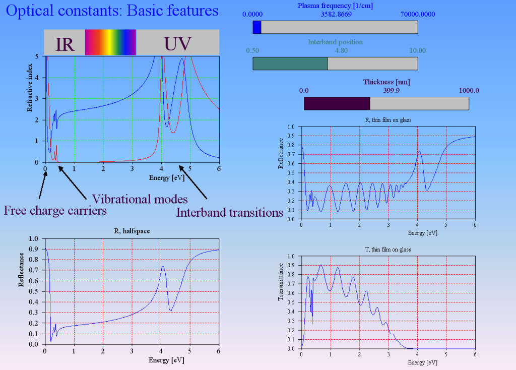
Optical constant models describe the response of matter to the electric fields of a light wave. The main mechanisms are
- acceleration of free charge carriers in conductive materials (free charge carrier absorption)
- exciting oscillations of bound charges (vibrational modes)
- lifting up electrons from an occupied electronic state to an empty state (interband transitions)
Interband transitions
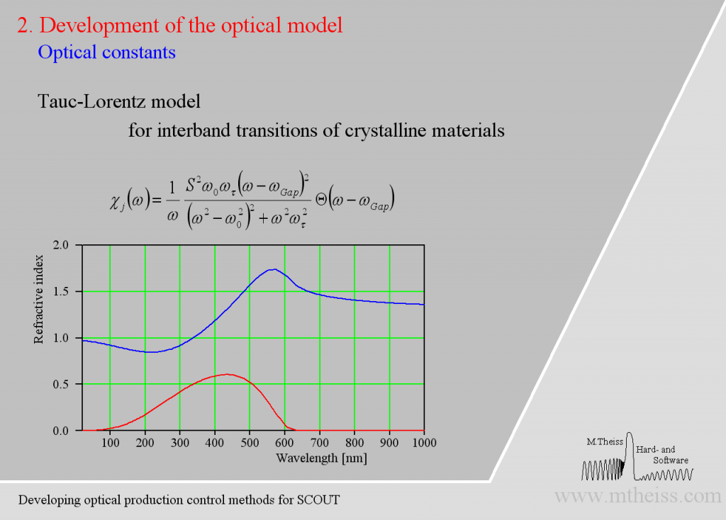
Electronic transitions can be roughly described by simple harmonic oscillators. However, these are not very realistic and should be used far away from the resonance frequency of the oscillator only. For band transitions of crystalline materials the Tauc-Lorentz model is appropriate:
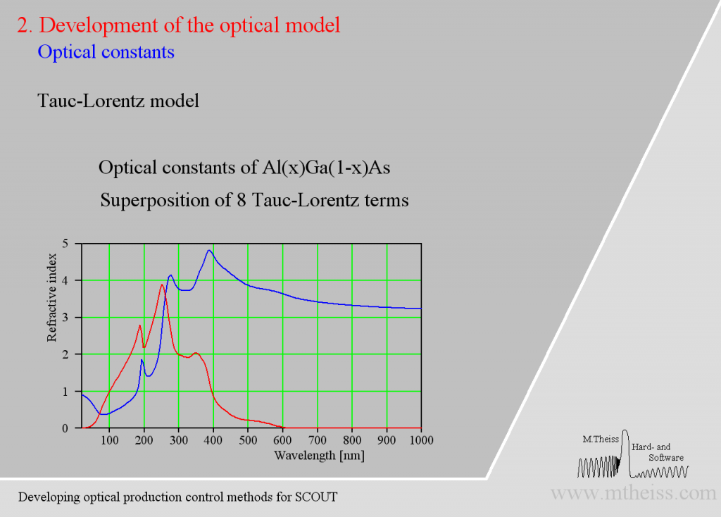
Be prepared to superimpose several of these terms since crystalline materials may have feature many interband transitions, like AlGaAs:
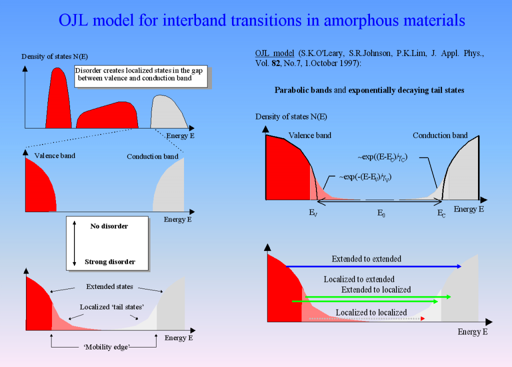
Amorphous semiconductors and almost all oxides and nitrides used in thin film applications can be described by the so-called OJL model. It is based on some very simple assumptions about the interband transition and states within the band gap which are caused by disorder:
For many materials the OJL model produces the correct shape of n and k with a few parameters only:
This makes fitting optical constants rather easy. In addition, the band gap parameter as well as the tail state exponent (also called ‘disorder parameter’) have physical meaning and characterize the state of the material.
Vibrational modes
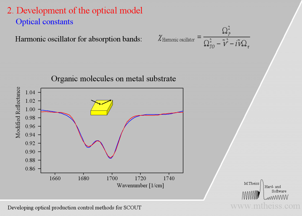
Although harmonic oscillators should be the right tool to describe vibrating parts of molecules or crystal lattices they are simplifying too much. Here is an attempt to describe 2 strong and a weak side band of molecules on a metal surface:
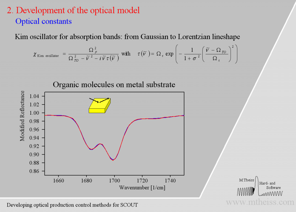
The model is ok but the overall shape of the absorption bands is not reproduced very well. The reason is that the harmonic oscillator has a constant damping parameter, i.e. the vibration is slowed down in the same way in the center (where the absorption is strong) as in the regions of small absorption. As the amplitude of whatever vibration we might have is certainly stronger in the resonance region the interaction with the outside world is certainly stronger. So whatever causes the damping will be stronger close to the resonance frequency and weaker far away from it – at least this is very likely. The so-called ‘Kim oscillator’ model uses a Gaussian decay of the damping with distance from the center of the oscillator and it fits many absorption bands very nicely, much better than the harmonic oscillator:
Besides describing vibrational modes the Kim oscillator can also model high energy interband transitions above the OJL model and the broad band absorption of confined charge carriers (which are almost free but are blocked to leave a microcrystal).
Free charge carrier excitation
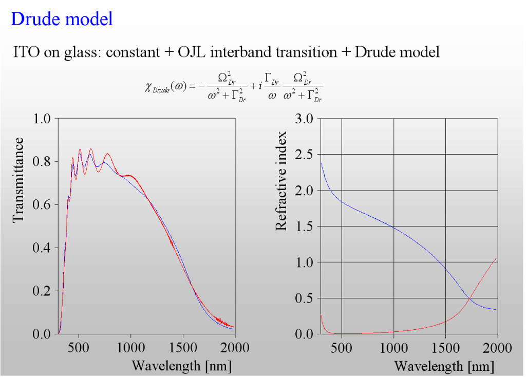
The absorption of light by the acceleration of free charges in a metal or doped semiconductor can be described by the classical Drude model. It has 2 parameters only – the plasma frequency is directly related to the concentration of charge carriers whereas the damping constant is connected to the mobility (or the inverse mean free path).
The only class of materials for which we need more than the Drude model is that of highly doped semiconductors, i.e. those materials which are used for transparent but conductive layers (TCOs). The following example shows the difference – the transmission spectrum of a ITO layer is not adequately reproduced by the (in this case too simple) Drude model:
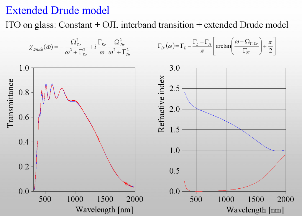
Again, like in the harmonic oscillator case, we need to introduce frequency dependent damping. As it turns out we need to have a smooth transition between 2 levels of damping – high in the mid infrared, and low in the near infrared:
The 3 extra parameters of this model describe the difference of the damping constants, the width as well as the spectral position of the transition zone.
For many applications TCOs need to be rather thick (a few hundred nm). Be prepared to face inhomogeneity in depth of such layers. In this case you need to use 2 or more sublayers which differ in the concentration of charge carriers.
Mixed materials
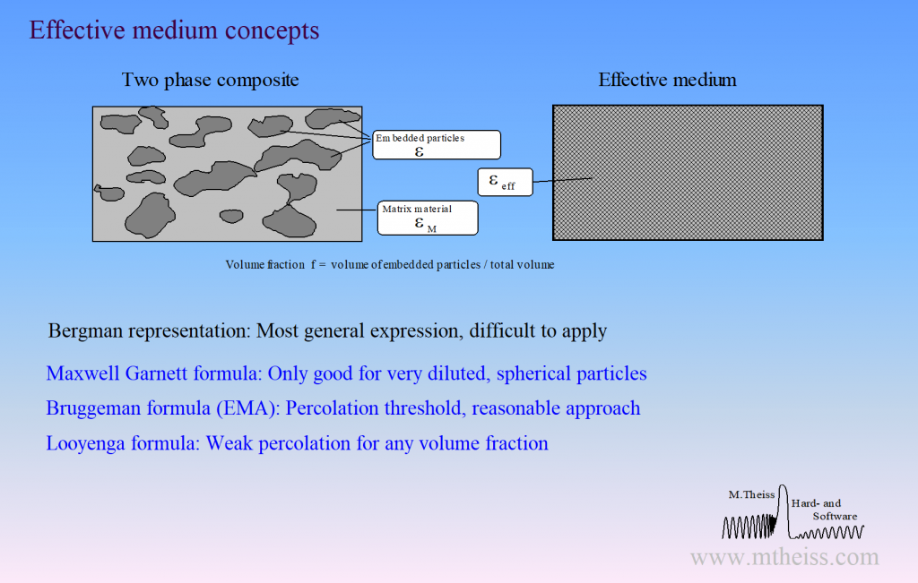
Surface roughness, porous materials or mixtures of 2 phases require the computation of effective optical constants.
Unfortunately, there is not a unique way of mixing optical constants. Our software packages have the following implementations for effective material properties:
- Bruggeman model (also known as EMA = Effective Medium Approximation)
- Maxwell Garnett model
- Looyenga model
- Bergman representation (very general, very powerful, but very difficult to apply). In fact, the Bergman representation includes all simple concepts, i.e. Bruggeman, Maxwell Garnett and Looyenga are special cases within the Bergman formalism.
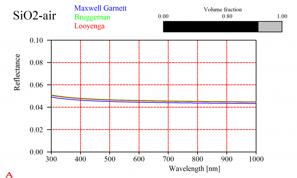
For some composites it does not really matter which approach you take. Here is the reflectance of a SiO2-air mixture, computed using the simple expressions given above:
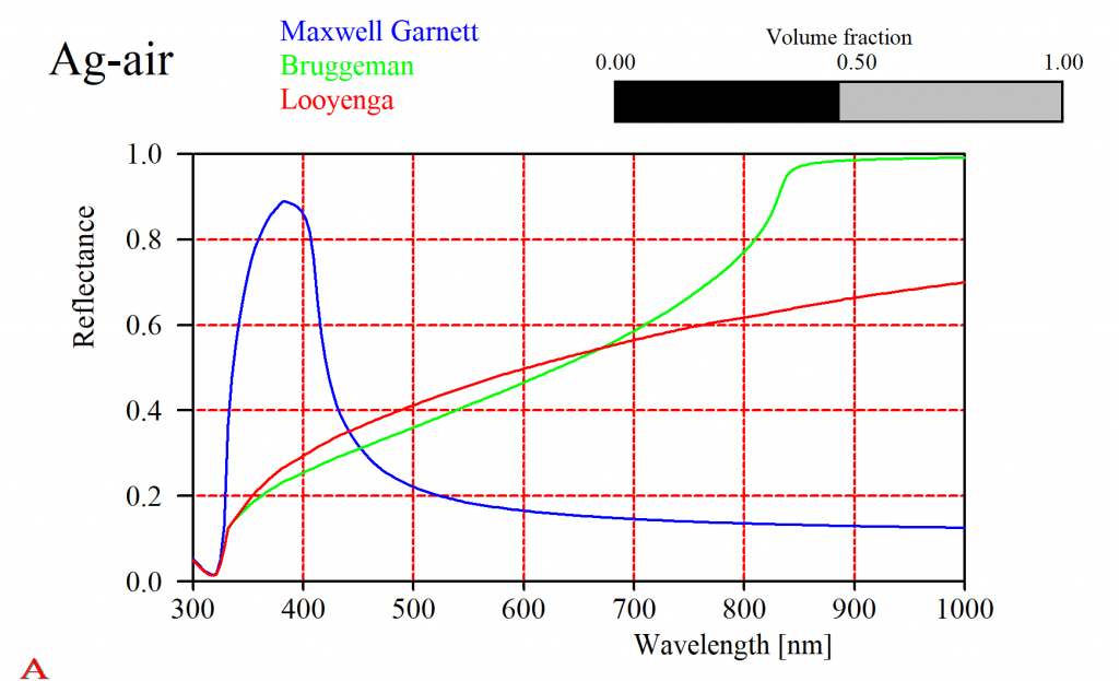
That should not lead to the wrong conclusion that this is always the case. Especially metals show a large variety of mixed properties. For a silver-air mixture the simple solutions give very different results (in fact, all of them will be quite wrong and you have to use the difficult Bergman approach):
Which model should I use?
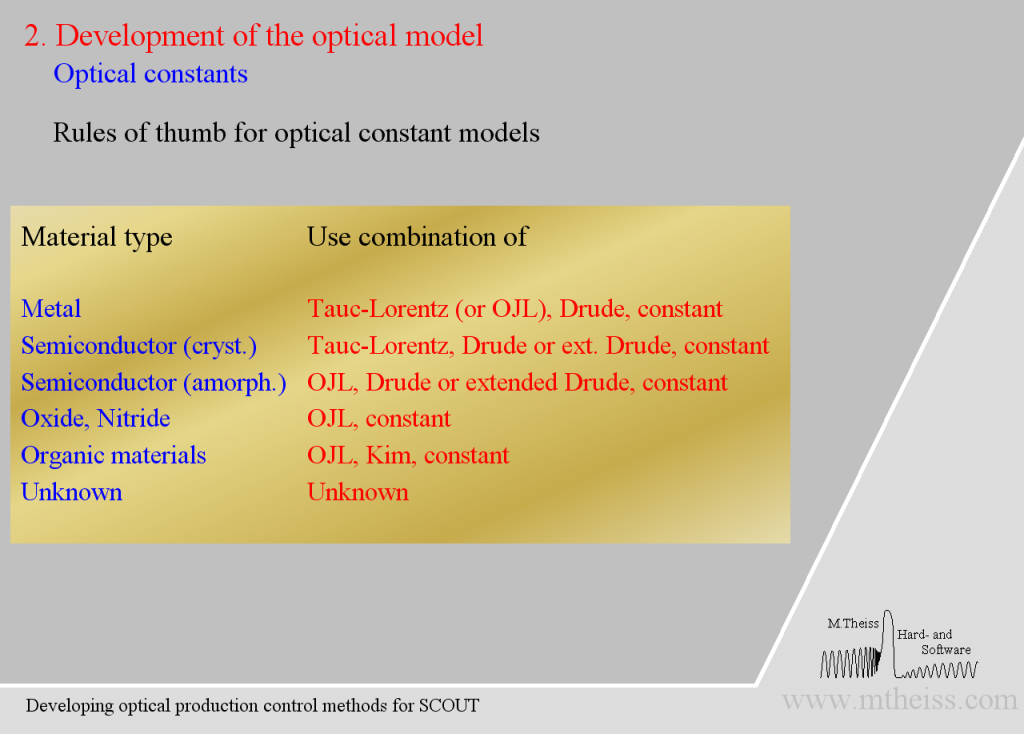
Finally, here are some recommendations which model to choose:
Emergency: Managed licenses don’t work – what to do?
New video platform
We have copied our tutorial videos to a second platform which is available in China. Click the following link:
WTheiss videos on alternative platform
MSVCP120.DLL is missing …
If you try to run CODE, SCOUT or SPRAY with object generation 4.50 or higher and you get this message please install the Visual C++ Redistributable package for Visual Studio 2013. Here is the link:
https://www.microsoft.com/en-us/download/details.aspx?id=40784
If you follow the ‘Download’ section you have to select the vcredist_x86.exe. Running this will install the required DLL files.
Object generation 4.29: Workbook export problem fixed
We have repaired the export of optical constants of some types of materials (in particular effective dielectric function objects) to the workbook.
New material object type: Interpolate n and k tables
We have introduced the above mentioned new type of material object in 2014 already. However, we forgot to add documentation to explain how to use it. This has been done now …
Here is the link to the updated SCOUT documentation page:
http://www.mtheiss.com/help/final/html/scout3/?motivation.htm
SPRAY help now online
Finally we have generated an online version of the SPRAY documentation. We recommend to use this source of information from now on – it will be updated most frequently.
Here is the link: SPRAY online help
New object computing absorption spectra
We have implemented a new type of detector: Objects of type ‘Absorbing material’ count rays which are absorbed in a selected material. After the ray-tracing the counts are normalized to the number of emitted rays. This results in an absorption spectrum.
Objects of this type can be used to measure absorption of light in objects which have a complex shape, like a silicon wafer with textured surfaces.
New wafer object
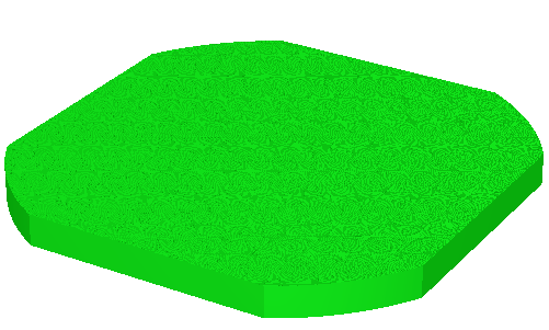
With SPRAY version 2.53 we have introduced a new geometric object called ‘wafer’ which represents a silicon wafer to be used in a solar cell. The wafer has a cylindrical base shape and is cut at the sides:
The bottom surface is textured with shapes that have been available in previous versions of SPRAY already.
The top surface can be textured the same way or using a new mechanism: In order to approach realistic textures you can now superimpose two textures which may have different shapes and periodicities. This opens a large variety of surface patterns (see examples below).
“Uniform” pyramids
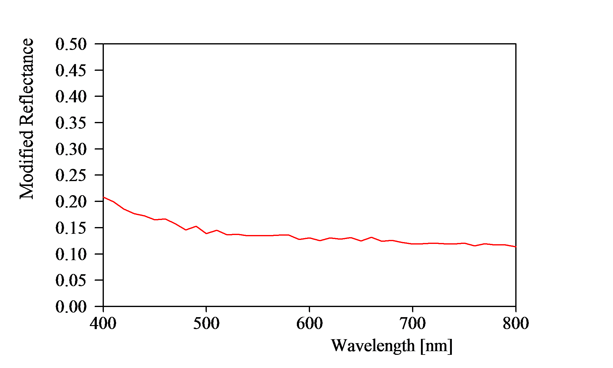
A surface texture of regular pyramids of one and the same size looks like this (for an inclination angle of 54°):
The reflectance spectrum in the spectral range 400 … 800 nm is this:
Average reflectance is 13.8%.
“Non-uniform” pyramids
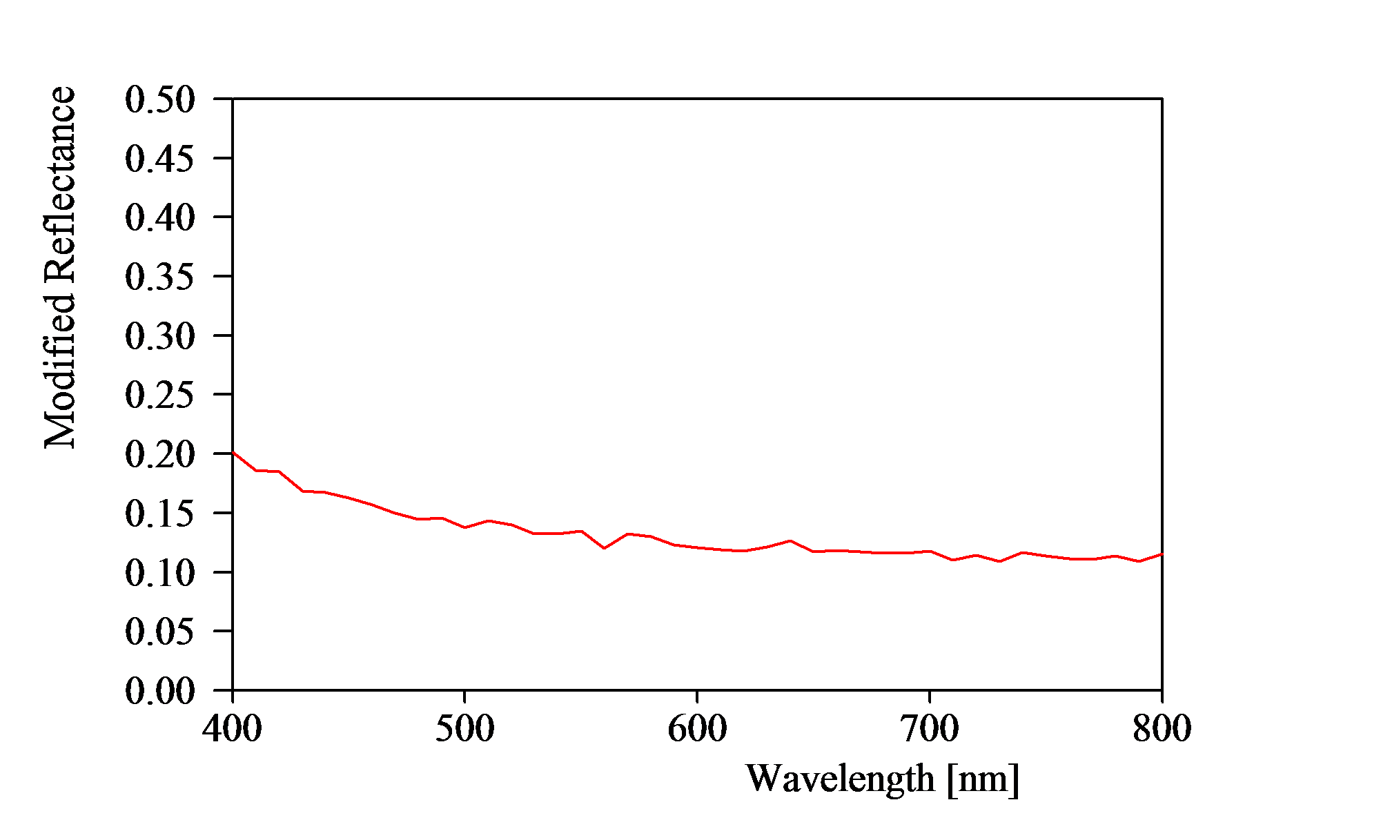
Big and small pyramids (with different heights and periodicities) mixed together:
Reflectance of this texture:
Average in the range 400 … 800 nm: 13.2%
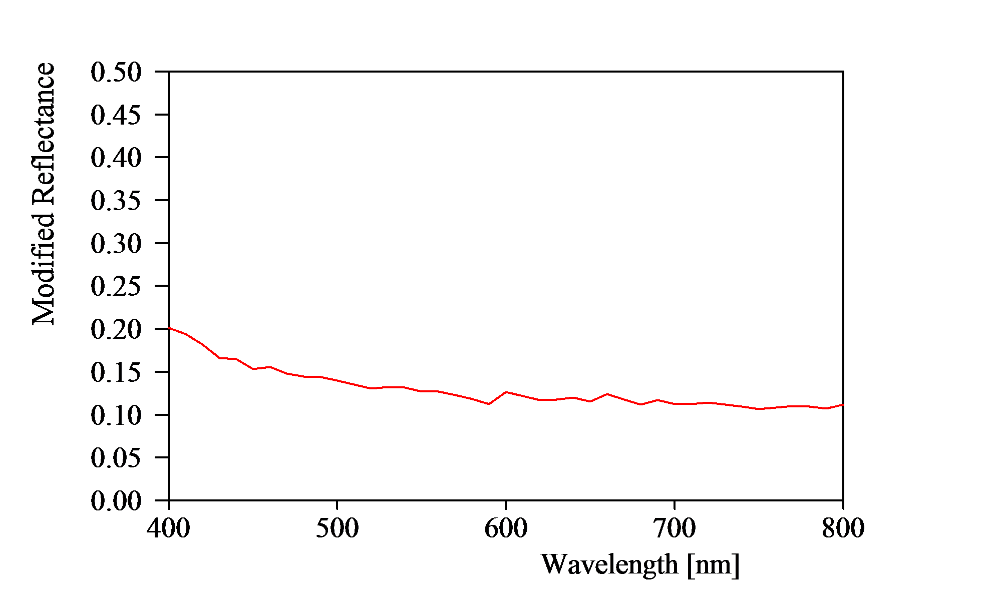
Big and medium sized pyramids mixed together – this looks quite realistic:
The reflectance of this kind of texture is this:
Average reflectance: 13.0%
You may assign different layer stacks to the bottom, side and top surfaces of the wafer object. This way you can introduce AR coatings on top which are not deposited at the sides and below.

