Category Archives: Optical modeling

Variation of 2 model parameters

We have updated the list of special computations. You can now do variations of 2 parameters rather easily, using objects of type ‘2 parameter variation’.

As an example we use a low-emission glass coating with several layers:

The goal of this exercise is to learn how the average transmittance in the visible (light transmittance) depends on the thickness values of the TiOx and SnOx layers. In our example configuration, the light transmittance is computed as third integral quantity:

To do the required computations we generate an object of type ‘2 parameter variation’ in the list of special computations:

Editing the new object brings up this dialog:

For each parameter you can select which one it is and how the range of values is chosen. The editor ‘Function to be evaluated’ allows to enter the quantity you want to compute for each pair of parameter values – in our case this is iq(3) (the light transmittance). If you check the option ‘Automatic export to workbook after computation’ the obtained data are written to the workbook.

Once this dialog is closed another one opens which is used to set graphics parameters for the graph of the data. This graph can be shown in a view if you drag the special computation object to a list of view items. The first parameter (TiOx in our case) will be displayed on the parameter axis, the second parameter values (SnOx thickness) will be displayed along the x-axis:

Please note: Computations may require some time for this type of object. Automatic updates are switched off which means you have to actively trigger the computation. You can do that in the list of special computations by selecting the object and then click the ‘Update’ menu item. If you display the object in a view re-computation is triggered by a click on the view object. Be careful to click only when you really want to start a new computation!

The graph looks like this:

You can also select to generate false color plots which you can use to display a kind of contour graph:

As mentioned above you have the option to store the computed data to the workbook. If your object is called ‘LT chart’ a workbook page with this name is created and the data are written to the worksheet, including minimum and maximum value as well as the position of these extrema:

CODE: Using measured sheet resistance values in batch fitting

Besides optical spectra CODE computes sheet resistance values of layers stacks. A sheet resistance object in the list of integral quantities computes the current value and – with the ‘Optimize’ option turned on – the squared difference to a given target value.

If you type in a measured sheet resistance value as target value CODE optimizes a layer stack to reproduce measured electrical performance (only if the option ‘Optimize’ is switched on, of course). If you check the option ‘Combine fit deviation of integral quantities and spectra’ (File/Options/Fit) you can fit spectra and sheet resistance at the same time, balancing importance by setting proper weights for each quantity.

We have now added the ability to take into account measured sheet resistance values to batch fitting. In order to use this new feature you have to define a sheet resistance object in the list of integral quantities and name it ‘sheet resistance fit’. Set its ‘Optimize’ option ‘On’. Then generate a new batch fit based on the current model – or use an existing one. Here is an example of the results page:

Note the empty line between the last spectrum (‘Reflectance’ in this case) and the line called ‘Fit’. Enter the key phrase ‘sheet resistance fit’ into the first column and type in or copy the measured values for each sample (i.e. for each column). The table should look like this now:

That’s all – you are now ready to start batch fitting. For each sample the measured values will be entered as target values and CODE will optimize both spectra and sheet resistance values.

You might encounter the difficulty that measured and simulated sheet resistance values do not easily agree. In this case you should check if your sample might show a depth gradient of the conductivity. A reason could be a depth dependent density of defects like grain boundaries within the layer. In such a case you should consider dividing the conductive layer into several parts with different damping constants of the charge carriers. You can read a discussion for silver and other conductive layers here.

Optimizing thin film solar cells with CODE

With CODE you can compute the photocurrent in an active layer of a solar cell. The photocurrent is available as integral quantity which can be the target of the layer stack optimization – very likely the target is ‘as high as possible’. Photocurrent objects make use of a special spectrum type in CODE which is called ‘Charge carrier generation’. Since the required steps to setup such a computational scheme are non-trivial (and a little bit hidden in the documentation) we have generated this tutorial which explains all details.

The example is a thin film solar cell with 2 active layers. One is micro-crystalline (mc-Si) and the other one amorphous (a-Si). Light enters through glass from the top. Between glass and the absorber layers a transparent conductive layer (TCO) collects charge charriers. The backside contact is made of aluminum.

The reflectance of the stack is easily calculated – this is standard in CODE:

If you are interested how much light is absorbed in one of the active layers you have to generate a spectrum of type ‘Layer absorption’ in the list of spectra. Please note that this spectrum type works for layer stacks which consist of either ‘thick layers’ or ‘thin films’ – you should not have ‘rough interface’ or ‘thickness averaging’ layers in the stack.

‘Layer absorption’ objects require the selection of the active layer. A control element for this is available in the upper left corner:

In addition, you have to set a parameter called ‘Number of sources’. CODE divides the layer of interest into several sublayers and computes the local electric field inside each sublayer. Then the absorbed power is computed and added up for all sublayers. ‘Number of sources’ is the number of sublayers – it should be selected high enough so that the final results do not change significantly if you change the number of sources somewhat.

In our example the fraction of light absorbed in the a-Si layer is this:

What really counts for the performance of the solar cell is the number of electron-hole pairs generate by the absorbed light. Not every photon may generate an electron-hole pair that contributes to the current of the cell. The spectrum type ‘Charge carrier generation’ is used here: It works like the type ‘Layer absorption’ discussed above, but multiplies the absorbed fraction by an internal efficiency function.

Each spectrum of type ‘Charge carrier generation’ has subobjects called ‘Local absorption’ and ‘Generation efficiency’. The local absorption subobject shows the local absorption of light within the stack:

Starting at z=0 on the left we see the absorption within the Al layer, followed by the a-Si and mc-Si absorption. Finally, on the right side, the TCO absorbs in the UV and the NIR.

The subobject ‘Generation efficiency’ is used to define the spectral function that returns the probability of the generation of an electron-hole pair by the absorption of a photon. Per default setting the internal efficiency is one:

However, you can click on ‘Definition’ to open a list that allows more flexibility:

In this list you can define a spectral dependence of the generation efficiency, using terms that you usually use for dielectric functions. You can use oscillators like this one:

Or a superposition of many oscillators or any user-defined function. The parameters of each term show up as potential fit parameters – this allows to tune the model and get some information about the generation process.

For simplicity in this example the internal efficiency is 1.0.

Having defined ‘Charge carrier generation’ objects for both active layers (mc-Si and a-Si) CODE knows the relation of absorbed photons and generated electron-hole pairs for each wavelength. In order to compute a macroscopic property we have to integrate over the whole spectrum. This is done by objects of type ‘photocurrent’ in the list of integral quantities. For each active layer you have to define one photocurrent object and assign the proper spectrum:

Editing a photocurrent object you can define the spectrum of the incident light and its integrated, total power. Please note that CODE uses the unit mA/cm^2 for the current density:

Next you have to define the spectrum of the incident radiation. Should the graph be missing press ‘Update’ to see it – or press ‘a’ on your keyboard for automatic scaling. Our example uses an AM1.5 spectrum. Do not worry about normalization – CODE will do that for you. You just have to provide the wanted spectral shape:

Finally, the total power of the illumination is entered in W/m^2:

Now CODE knows all parameters and computes the current density generated in the active layer.

In our example we have 2 active layers which may have different layer absorption and also different current densities:

Depending on layer thickness values one or the other active layer produces more current. You can generate graphs like the following doing a parameter variation (which generates all data in the workbook) and a view element showing workbook data:


What makes the difference between a good and a very good optical model?

Answering some recent questions about optical modelling, I dug out some old slides. They explain some model improvements that were implemented a long time ago. Combined with today’s fast computer hardware they provide the basis of high quality modelling.

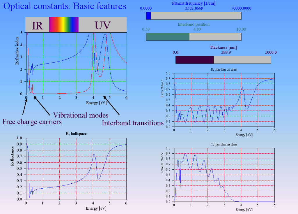
Optical constant models describe the response of matter to the electric fields of a light wave. The main mechanisms are

  • acceleration of free charge carriers in conductive materials (free charge carrier absorption)
  • exciting oscillations of bound charges (vibrational modes)
  • lifting up electrons from an occupied electronic state to an empty state (interband transitions)

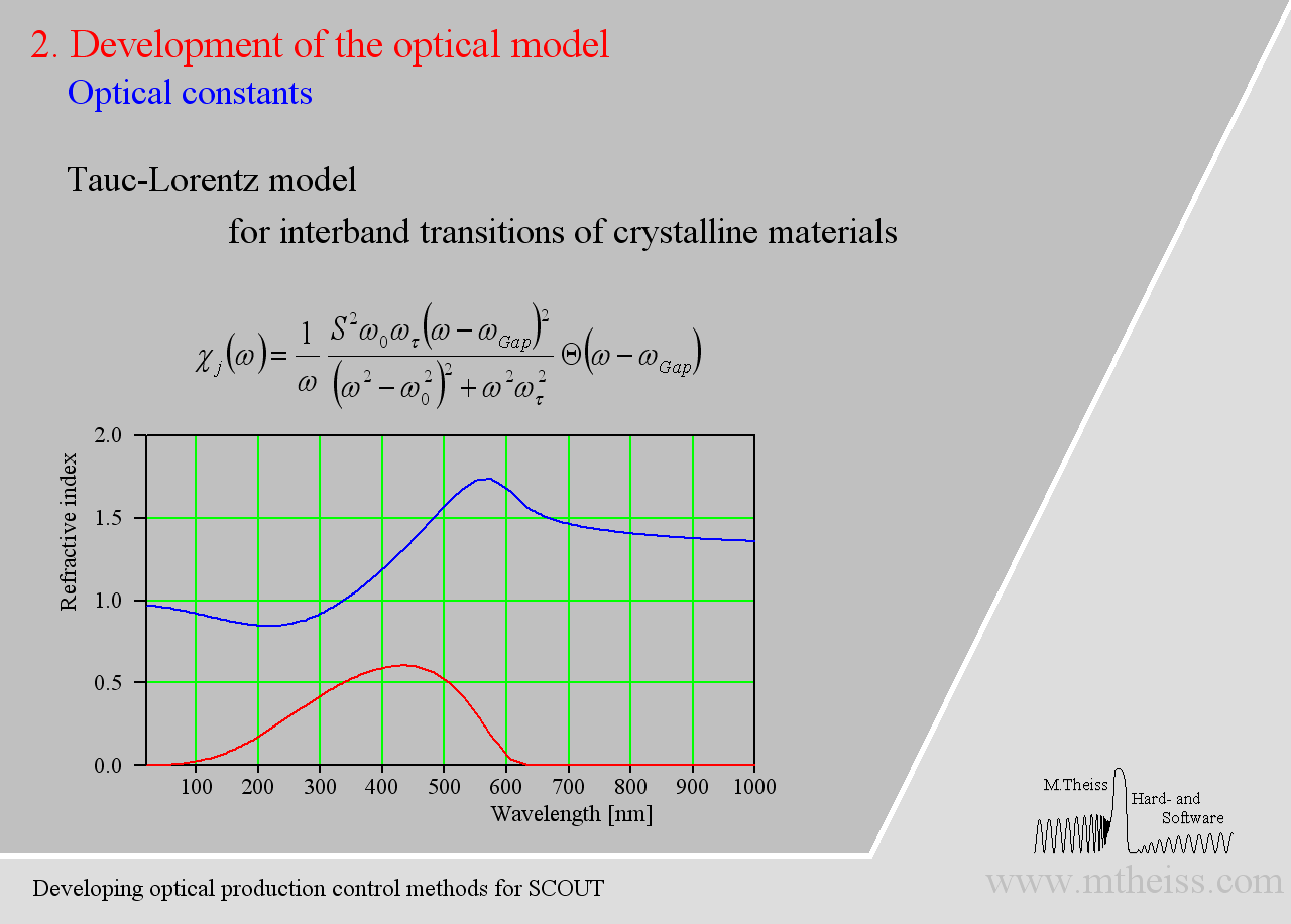
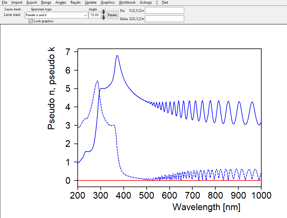
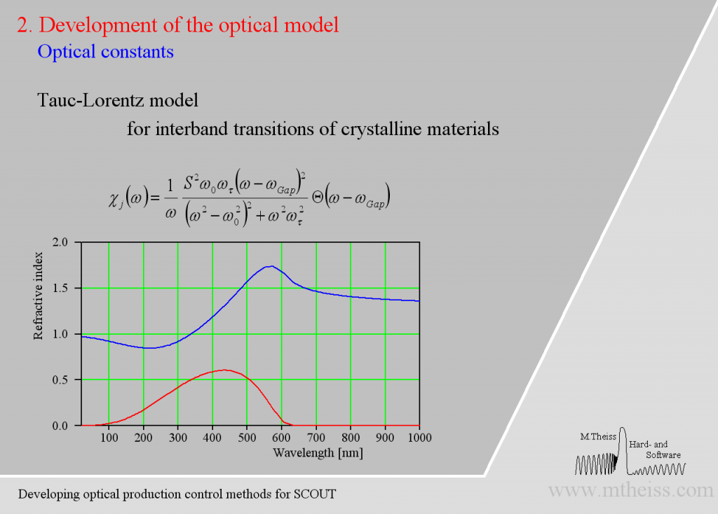
Interband transitions

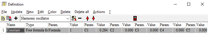
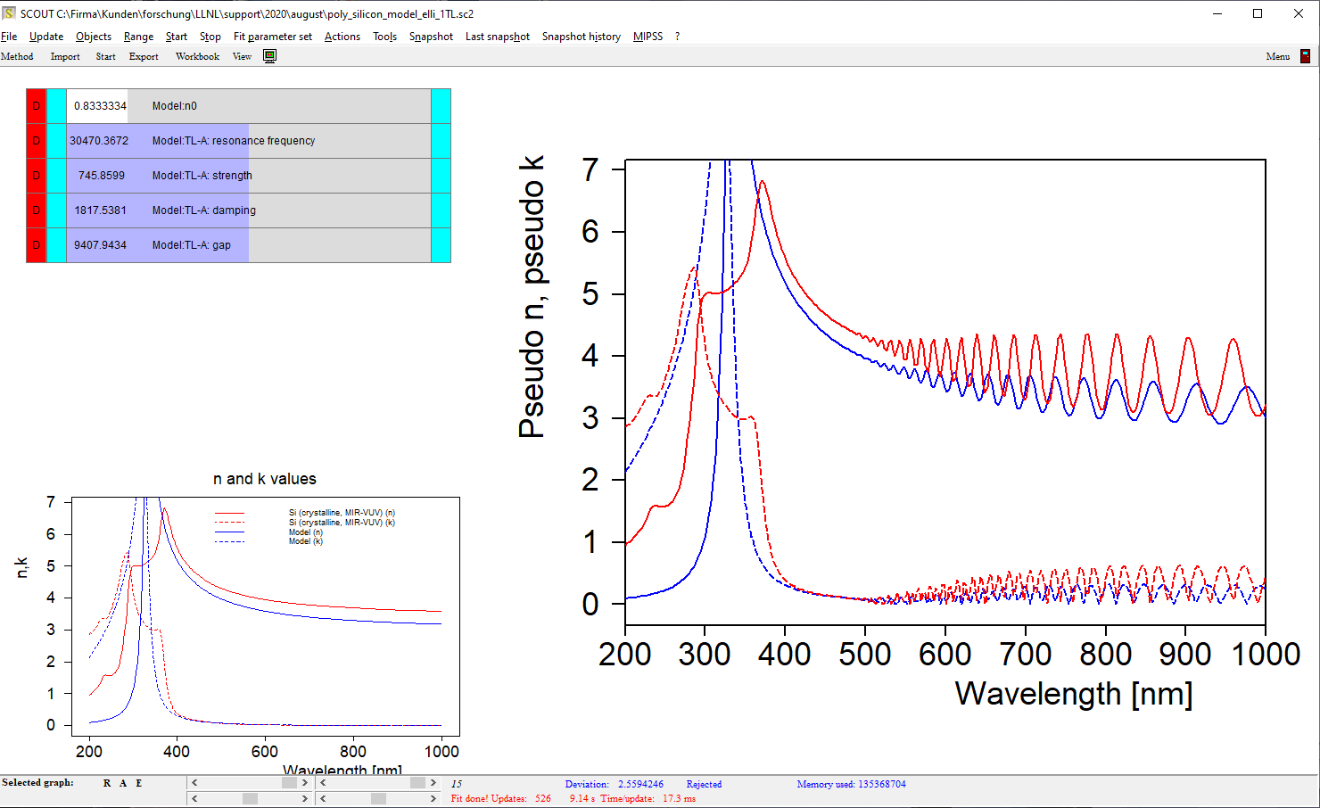
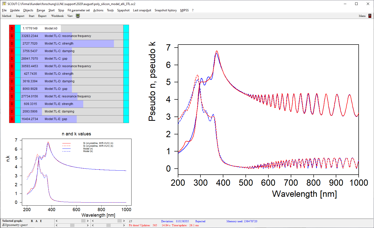
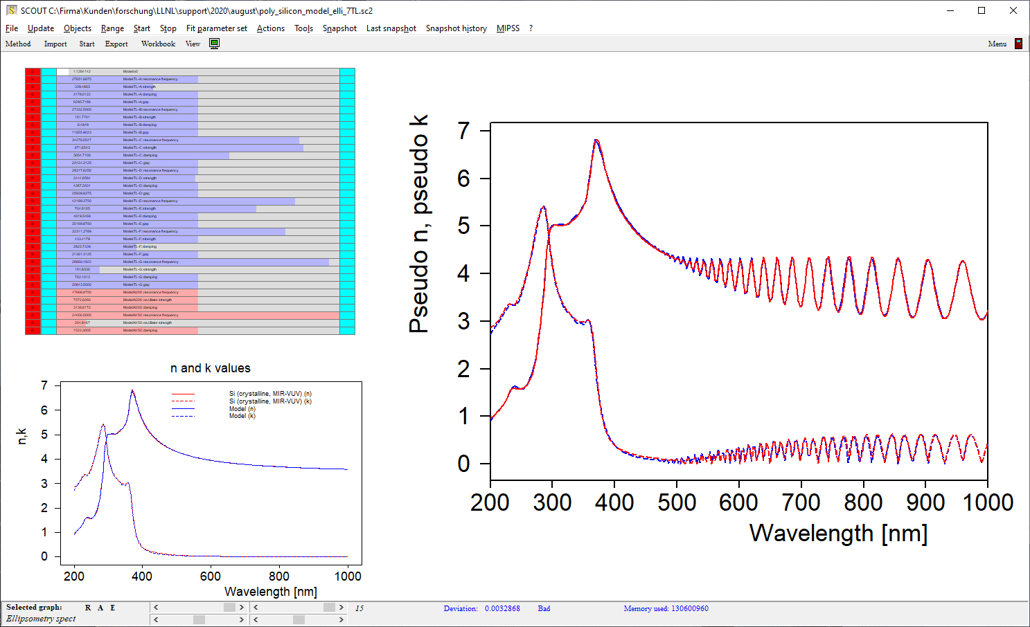
Electronic transitions can be roughly described by simple harmonic oscillators. However, these are not very realistic and should be used far away from the resonance frequency of the oscillator only. For band transitions of crystalline materials the Tauc-Lorentz model is appropriate:

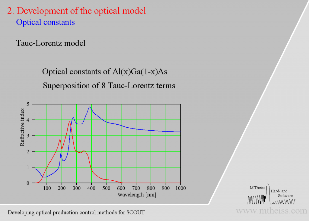
Be prepared to superimpose several of these terms since crystalline materials may have feature many interband transitions, like AlGaAs:

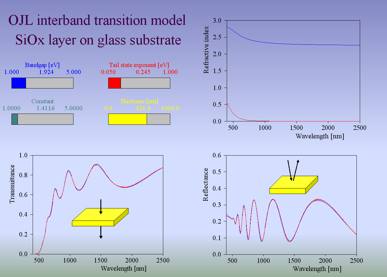
Amorphous semiconductors and almost all oxides and nitrides used in thin film applications can be described by the so-called OJL model. It is based on some very simple assumptions about the interband  transition and states within the band gap which are caused by disorder:

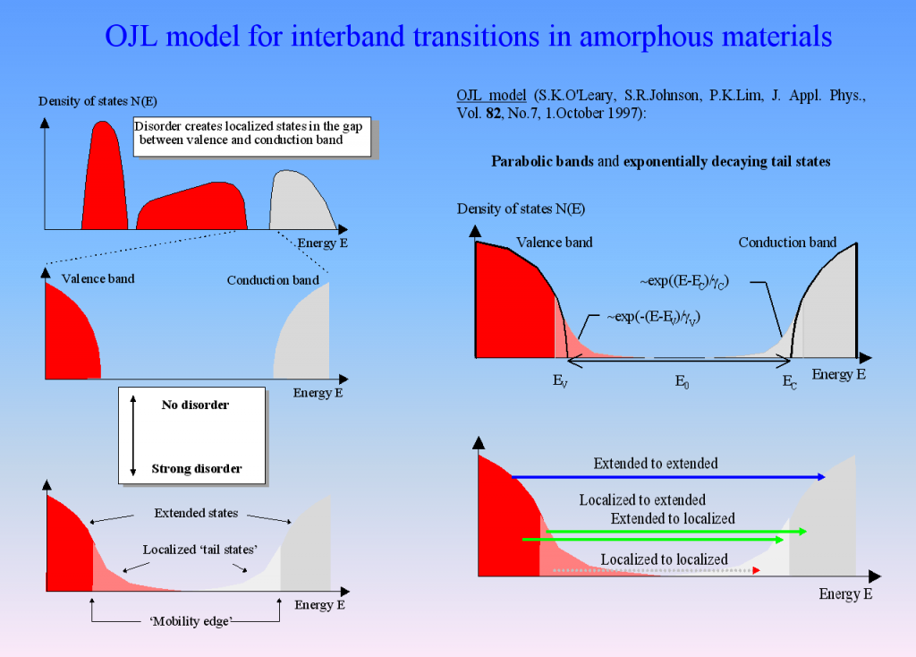
For many materials the OJL model produces the correct shape of n and k with a few parameters only:

This makes fitting optical constants rather easy. In addition, the band gap parameter as well as the tail state exponent (also called ‘disorder parameter’) have physical meaning and characterize the state of the material.
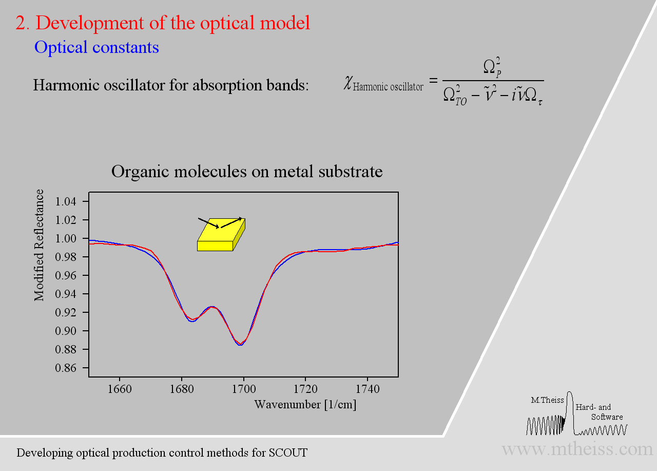
Vibrational modes

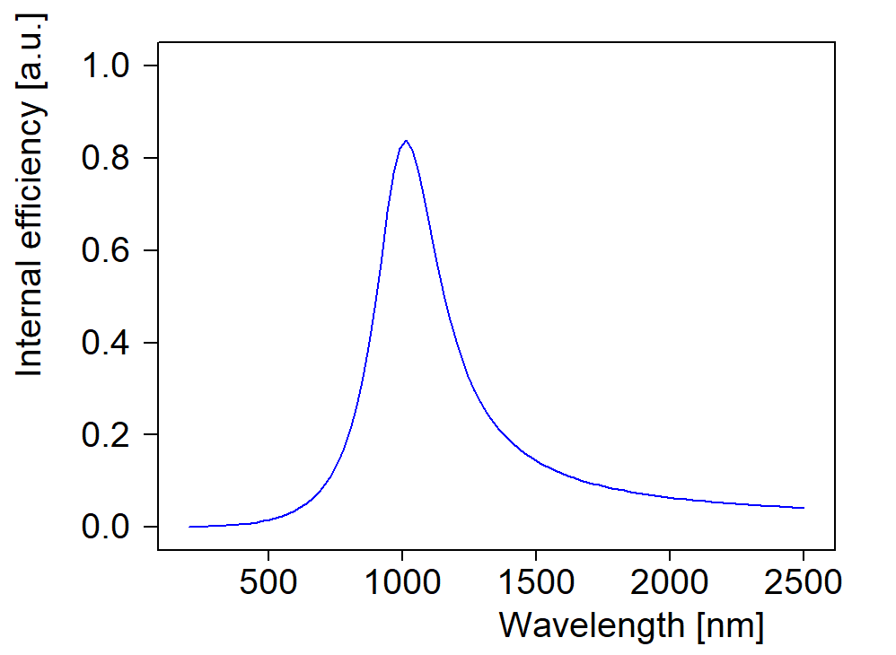
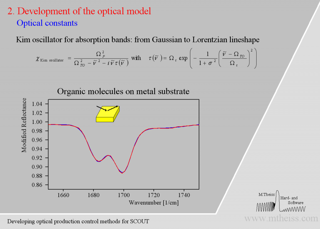
Although harmonic oscillators should be the right tool to describe vibrating parts of molecules or crystal lattices they are simplifying too much. Here is an attempt to describe 2 strong and a weak side band of molecules on a metal surface:

The model is ok but the overall shape of the absorption bands is not reproduced very well. The reason is that the harmonic oscillator has a constant damping parameter, i.e. the vibration is slowed down in the same way in the center (where the absorption is strong) as in the regions of small absorption. As the amplitude of whatever vibration we might have is certainly stronger in the resonance region the interaction with the outside world is certainly stronger. So whatever causes the damping will be stronger close to the resonance frequency and weaker far away from it – at least this is very likely. The so-called ‘Kim oscillator’ model uses a Gaussian decay of the damping with distance from the center of the oscillator and it fits many absorption bands very nicely, much better than the harmonic oscillator:

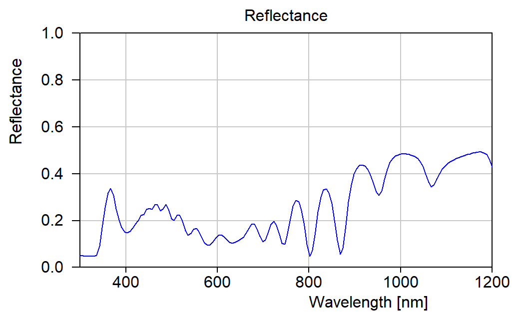
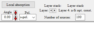
Besides describing vibrational modes the Kim oscillator can also model high energy interband transitions above the OJL model and the broad band absorption of confined charge carriers (which are almost free but are blocked to leave a microcrystal).

Free charge carrier excitation

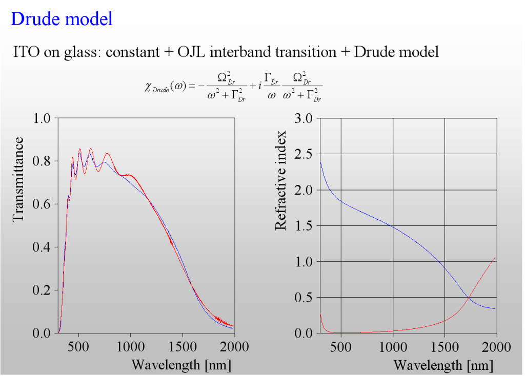
The absorption of light by the acceleration of free charges in a metal or doped semiconductor can be described by the classical Drude model. It has 2 parameters only – the plasma frequency is directly related to the concentration of charge carriers whereas the damping constant is connected to the mobility (or the inverse mean free path).

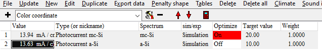
The only class of materials for which we need more than the Drude model is that of highly doped semiconductors, i.e. those materials which are used for transparent but conductive layers (TCOs). The following example shows the difference – the transmission spectrum of a ITO layer is not adequately reproduced by the (in this case too simple) Drude model:

Again, like in the harmonic oscillator case, we need to introduce frequency dependent damping. As it turns out we need to have a smooth transition between 2 levels of damping – high in the mid infrared, and low in the near infrared:

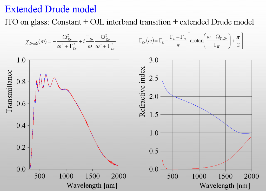
The 3 extra parameters of this model describe the difference of the damping constants, the width as well as the spectral position of the transition zone.

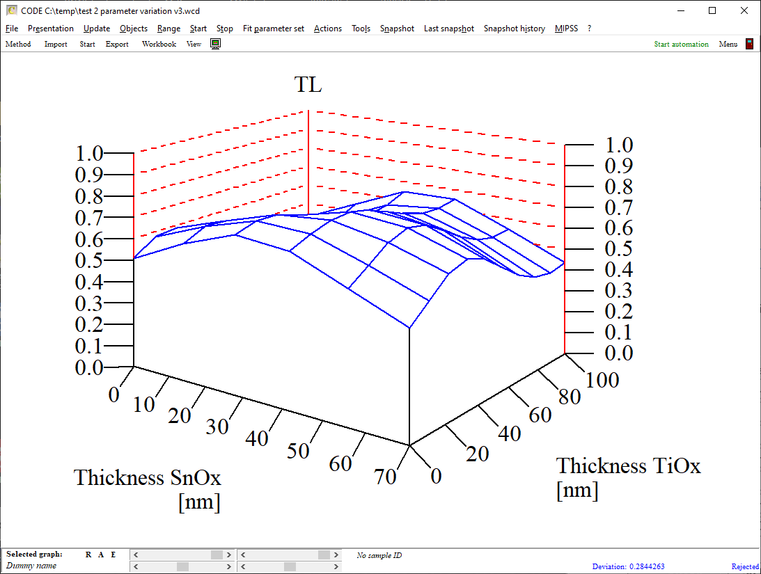
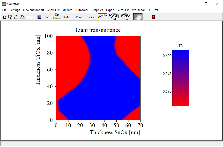
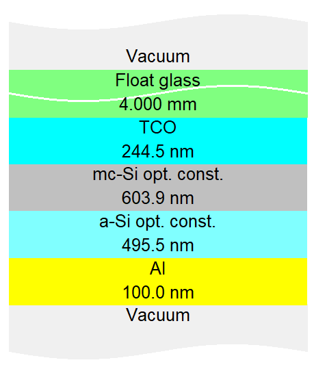
For many applications TCOs need to be rather thick (a few hundred nm). Be prepared to face inhomogeneity in depth of such layers. In this case you need to use 2 or more sublayers which differ in the concentration of charge carriers.
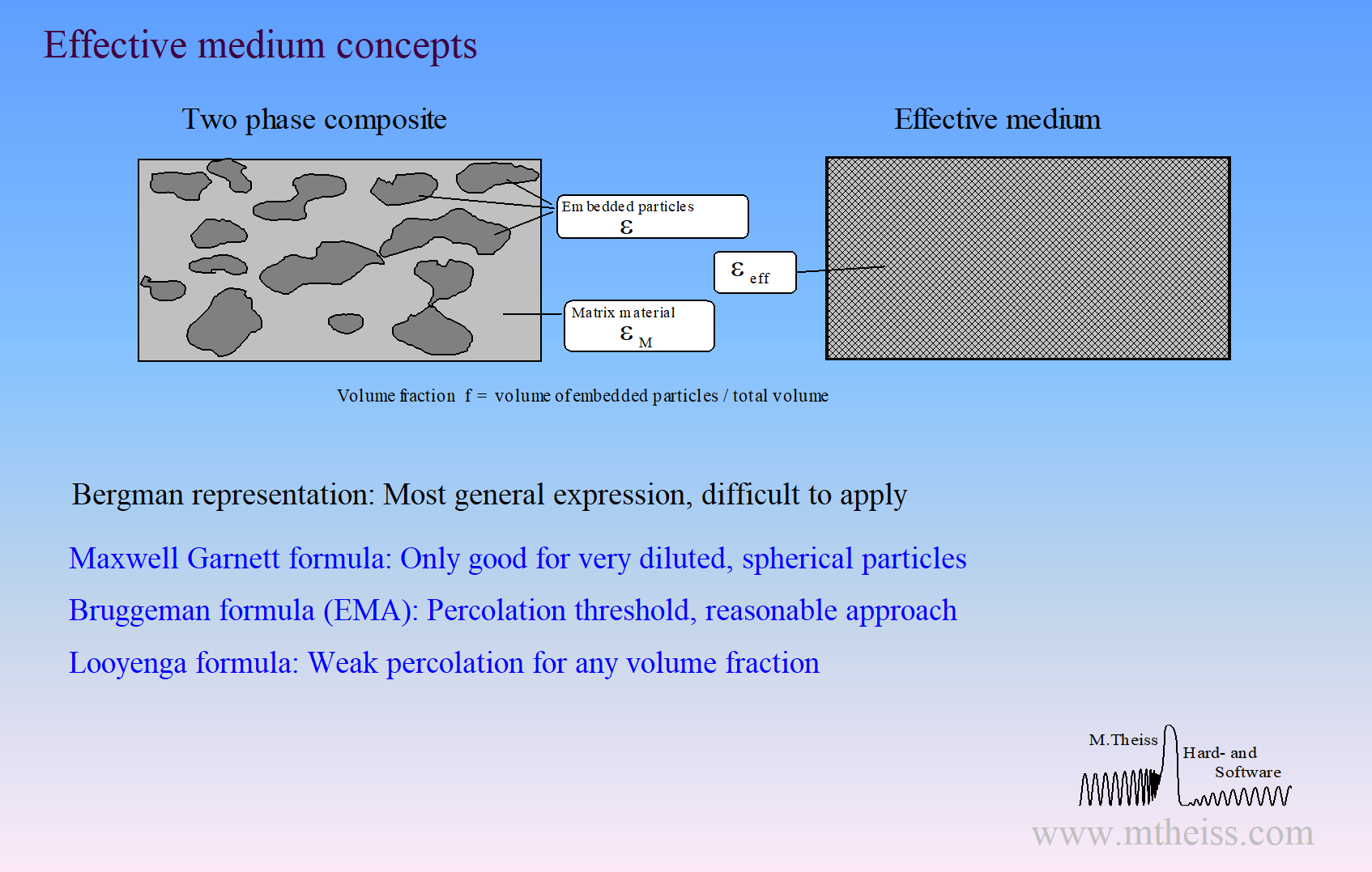
Mixed materials

Surface roughness, porous materials or mixtures of 2 phases require the computation of effective optical constants.

Unfortunately, there is not a unique way of mixing optical constants. Our software packages have the following implementations for effective material properties:

  • Bruggeman model (also known as EMA = Effective Medium Approximation)
  • Maxwell Garnett model
  • Looyenga model
  • Bergman representation (very general, very powerful, but very difficult to apply). In fact, the Bergman representation includes all simple concepts, i.e. Bruggeman, Maxwell Garnett and Looyenga are special cases within the Bergman formalism.

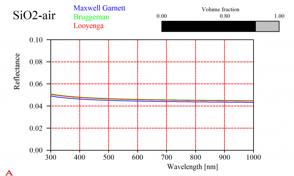
For some composites it does not really matter which approach you take. Here is the reflectance of a SiO2-air mixture, computed using the simple expressions given above:

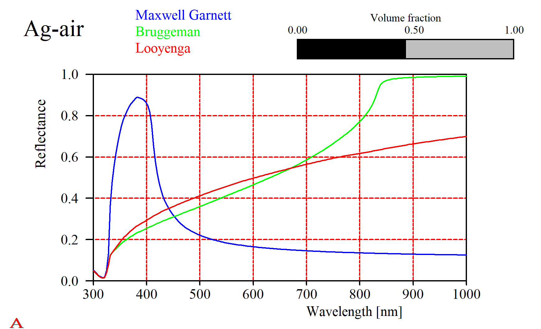
That should not lead to the wrong conclusion that this is always the case. Especially metals show a large variety of mixed properties. For a silver-air mixture the simple solutions give very different results (in fact, all of them will be quite wrong and you have to use the difficult Bergman approach):

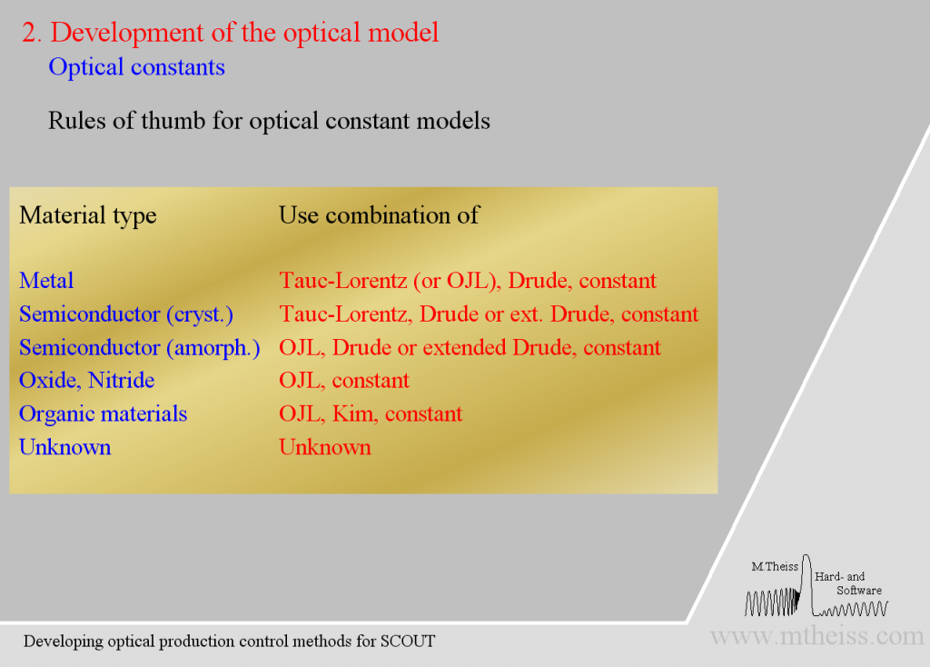
Which model should I use?

Finally, here are some recommendations which model to choose:


How to develop flexible optical constant models based on given n and k tables

Materials used in thin films may differ in their optical constants n and k from the corresponding bulk versions. Even if you find optical constant tables in literature for your application you may need to make some adjustments to the n and k values. This is certainly difficult if you have just a table of fixed values – what you need is a flexible model which can adjust the spectral shape of n and k by modifying a few key parameters only. This short tutorial shows how to proceed in such a case.

Crystalline silicon is used as example. The database of our SCOUT and CODE software packages contain several silicon versions. Here I have selected the item ‘Silicon (crystalline, MIR-VUV)’. These are the n and k data, featuring several interband transitions and a slow decay of k towards the indirect band gap around 1.1 eV:

If you change the temperature of a silicon wafer or deposit poly-crystalline silicon thin films you may observe similar structures but not exactly the same n and k – a flexible model would be nice to have. Our strategy to develop such a model will be this: First, we generate ‘measured data’ which are computed using the existing n and k table values. Then, in the second step, we setup a suitable model and adjust its parameters to reproduce the ‘measured’ data. If the ‘measurements’ provide enough information the n and k values of the model should be almost the same as those of the original table.

Since we will simulate the measurements we can easily work with a system which would be almost impossible to realize. In order to clearly ‘see’ the weak silicon absorption in the visible we use a 2 micron thick free standing layer – this layer is quite transparent and it will generate a nice interference pattern. To match the amplitude of the fringes will be difficult with wrong k values – so this setup ensures good n and k data of the model in the visible and NIR. The layer stack is this:

Using this layer stack we could now generate several reflectance and transmittance spectra, taken at various angles of incidence. This would make a nice set of ‘measured data’ for the fit procedure. However, to make our life as easy as possible we can use an ellipsometry object in the list of spectra. Objects of this type have the option to compute so-called ‘Pseudo n and k’ values. With this option the ellipsometric angles Psi and Delta are represented by pseudo n and k values of a virtual single interface. In spectral regions where our silicon layer is opaque the pseudo n and k values are the same as the real ones. In the transparent region the pseudo n and k values reflect the interference structures – this looks strange, and one could certainly question the usefulness of the concept ‘Pseudo n and k’. However, the interference pattern is what we go for to get good small k values in the model. The blue curves below show the generated pseudo n and k values. Within this example we will work in the spectral range 200 … 1000 nm:

Ellipsometry objects offer the local menu command ‘Actions / Use simulated data as measured data’ which is what we need now. The blue curves are now copied to the red measurement data as if we had imported measured data.

We can now replace the material object by our first model in the layer stack. I have started with a very simple model which consists of a constant real part of the refractive index and a Tauc-Lorentz model (inside a KKR susceptibility object). It is a good idea to generate a new item of type ‘Multiple spectra view’ which can show both the original table values of n and k and the model values in one graph (lower left side). With this simple model, you cannot expect a good match since  silicon shows several interband transitions in the range 200 … 1000 nm:

However, if we limit the range to 400 … 1000 nm the simple model works quite well:

For the full range (200 … 1000 nm) we need more interband transitions. Sticking to the Tauc-Lorentz oscillator type, I have added 2 more which brings up to a new level (still not satisfying, though):

Depending on your patience (and the needs of the final application) you can add more features as you like, approaching the former table values of n and k more and more. I stopped my example at this level:

The model developed for silicon this way can now be saved to the optical constant database for future use. You can use it for studies of systematic variations of deposition conditions and generate tables like ‘resonance frequency vs deposition temperature’.

You can follow the strategy shown in this tutorial for all kinds of materials, as long as you get good tabulated values of n and k to start with.

Polarizer for R and T measurements

We have added a polarizer to our desktop R and T measurement system. The same polarizer can be used for all systems recording R and T for shiny, non-scattering samples.

The desktop system records the 100% signal when detector and light source are positioned directly opposite to each other:

After this measurement you can do absolute reflectance measurements at arbitrary angles of incidence. We have generated tools to conveniently set fixed angles of incidence – here we have used 45° and 60°.

The graph below shows 4 absolute spectra of a silicon wafer (45°, 60°, s- and p-polarization). We could achieve almost perfect match of simulated spectra based on literature data of the optical constants, fitting a thickness of 6.2 nm of the native SiO2 layer on the wafer. Data acquisition for each spectrum took less than 1 second (averaging 18 spectra using an integration time of 50 ms).

Angle of incidence distribution

Spectroscopic experiments can never realize single angle of incidence but have to work with a (continuous) distribution of angles. Although in most cases the assumption of a single angle of incidence is a very good approximation there are cases where we need to take into account more details in producing simulated spectra. One example is taking reflectance spectra of small spots with a microscope objective, using a large cone of incident radiation.

For a long time our software packages can compute spectra averaged for a set of incidence angles, each one defined by the value of the angle and a weight. We have now implemented new features to simplify work in this field.

If you have prepared a list of angles of incidence you can now connect these angles to the angle of incidence that you have defined for spectrum object which owns the list of angles. You can check the option as shown here:

If you have activated this option you can use a set of angles with positive and negative values (centered around 0) as shown here:

If the angle of the parent object is 50° the computation of the spectrum is done for the 3 angles 45°, 50° and 55°, with weights 0.3, 0.4 and 0.3, respectively. If you have declared the angle of the parent object to be a fit parameter the set of 3 angles is moved automatically when the value of the center angle changes during the fit. This helps to adjust the distribution of angles to match the experimental settings.

Finally, there is a new fit parameter called ‘Scaling factor of angle range’. This number scales the distance of the individual angles to the center angle: If the factor is 1.0 the original angles are used. If the factor is 0.1, for example, a value of 5° becomes 0.5°. Varying the factor between 0.1 and 2 in the example shown above, you can compute spectra for a distributions between -0.5° … 0.5° to -10° … 10°.

We hope that this new flexibility helps to achieve better fitting results for spectra measured with microscopes or other systems with spectra features depending critically on the angle of incidence.