Materials used in thin films may differ in their optical constants n and k from the corresponding bulk versions. Even if you find optical constant tables in literature for your application you may need to make some adjustments to the n and k values. This is certainly difficult if you have just a table of fixed values – what you need is a flexible model which can adjust the spectral shape of n and k by modifying a few key parameters only. This short tutorial shows how to proceed in such a case.
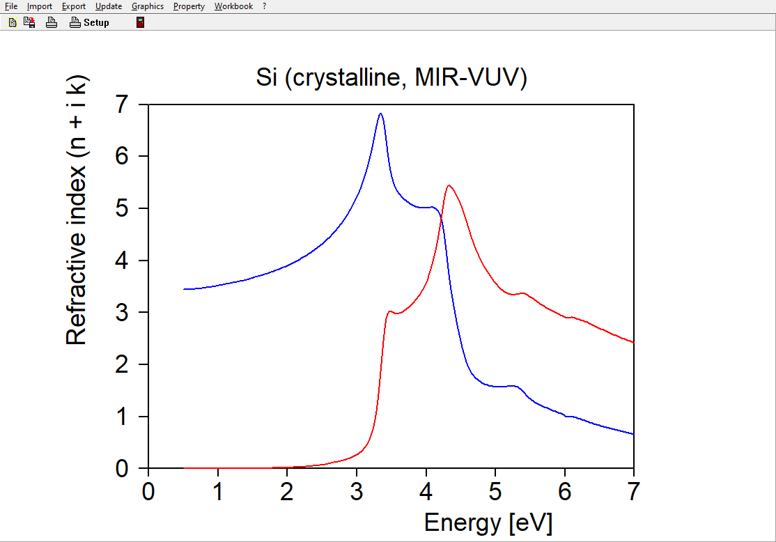
Crystalline silicon is used as example. The database of our SCOUT and CODE software packages contain several silicon versions. Here I have selected the item ‘Silicon (crystalline, MIR-VUV)’. These are the n and k data, featuring several interband transitions and a slow decay of k towards the indirect band gap around 1.1 eV:
If you change the temperature of a silicon wafer or deposit poly-crystalline silicon thin films you may observe similar structures but not exactly the same n and k – a flexible model would be nice to have. Our strategy to develop such a model will be this: First, we generate ‘measured data’ which are computed using the existing n and k table values. Then, in the second step, we setup a suitable model and adjust its parameters to reproduce the ‘measured’ data. If the ‘measurements’ provide enough information the n and k values of the model should be almost the same as those of the original table.
Since we will simulate the measurements we can easily work with a system which would be almost impossible to realize. In order to clearly ‘see’ the weak silicon absorption in the visible we use a 2 micron thick free standing layer – this layer is quite transparent and it will generate a nice interference pattern. To match the amplitude of the fringes will be difficult with wrong k values – so this setup ensures good n and k data of the model in the visible and NIR. The layer stack is this:

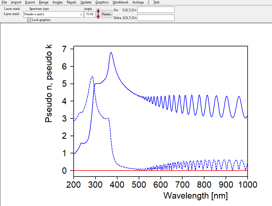
Using this layer stack we could now generate several reflectance and transmittance spectra, taken at various angles of incidence. This would make a nice set of ‘measured data’ for the fit procedure. However, to make our life as easy as possible we can use an ellipsometry object in the list of spectra. Objects of this type have the option to compute so-called ‘Pseudo n and k’ values. With this option the ellipsometric angles Psi and Delta are represented by pseudo n and k values of a virtual single interface. In spectral regions where our silicon layer is opaque the pseudo n and k values are the same as the real ones. In the transparent region the pseudo n and k values reflect the interference structures – this looks strange, and one could certainly question the usefulness of the concept ‘Pseudo n and k’. However, the interference pattern is what we go for to get good small k values in the model. The blue curves below show the generated pseudo n and k values. Within this example we will work in the spectral range 200 … 1000 nm:
Ellipsometry objects offer the local menu command ‘Actions / Use simulated data as measured data’ which is what we need now. The blue curves are now copied to the red measurement data as if we had imported measured data.
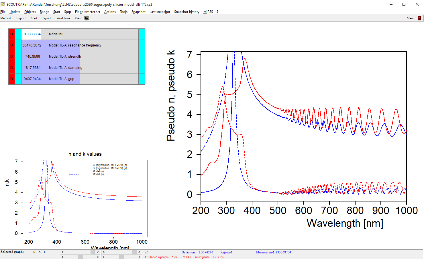
We can now replace the material object by our first model in the layer stack. I have started with a very simple model which consists of a constant real part of the refractive index and a Tauc-Lorentz model (inside a KKR susceptibility object). It is a good idea to generate a new item of type ‘Multiple spectra view’ which can show both the original table values of n and k and the model values in one graph (lower left side). With this simple model, you cannot expect a good match since silicon shows several interband transitions in the range 200 … 1000 nm:
However, if we limit the range to 400 … 1000 nm the simple model works quite well:
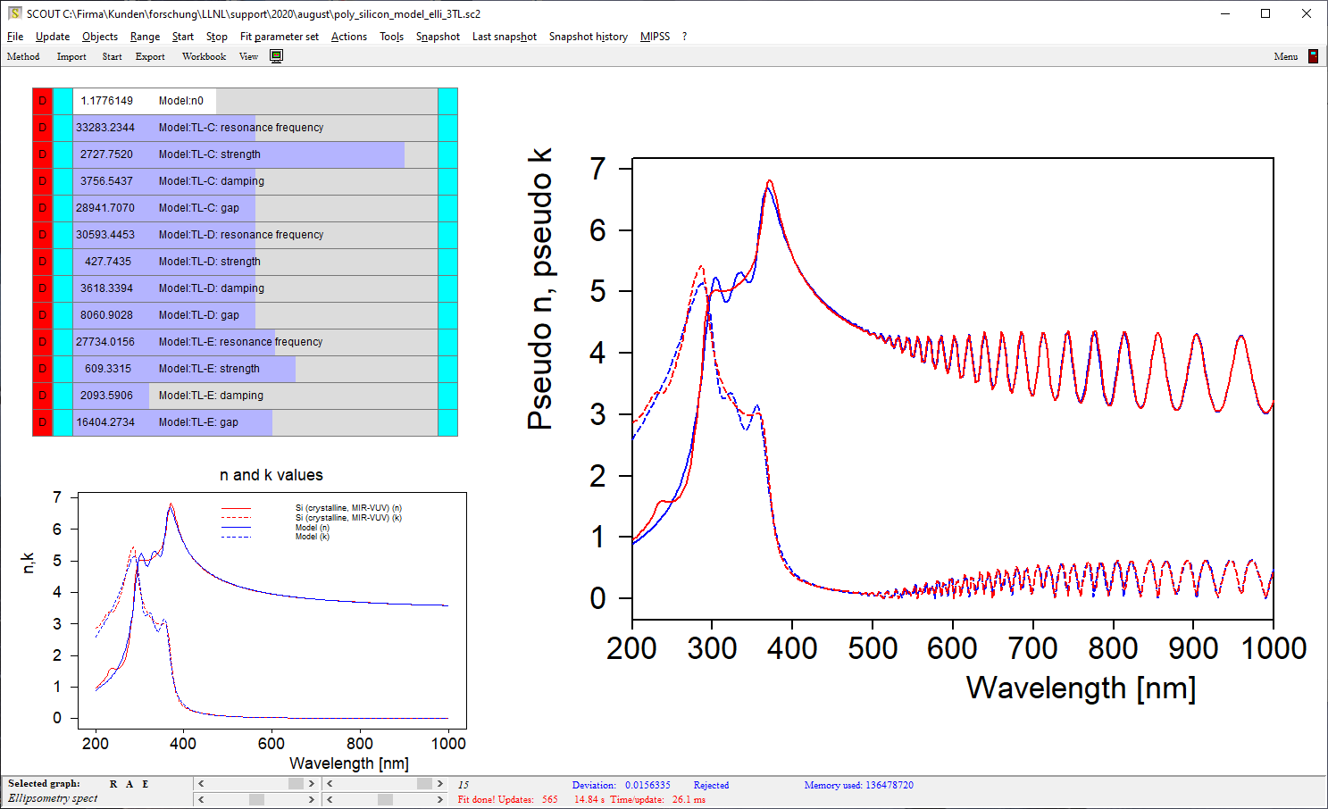
For the full range (200 … 1000 nm) we need more interband transitions. Sticking to the Tauc-Lorentz oscillator type, I have added 2 more which brings up to a new level (still not satisfying, though):
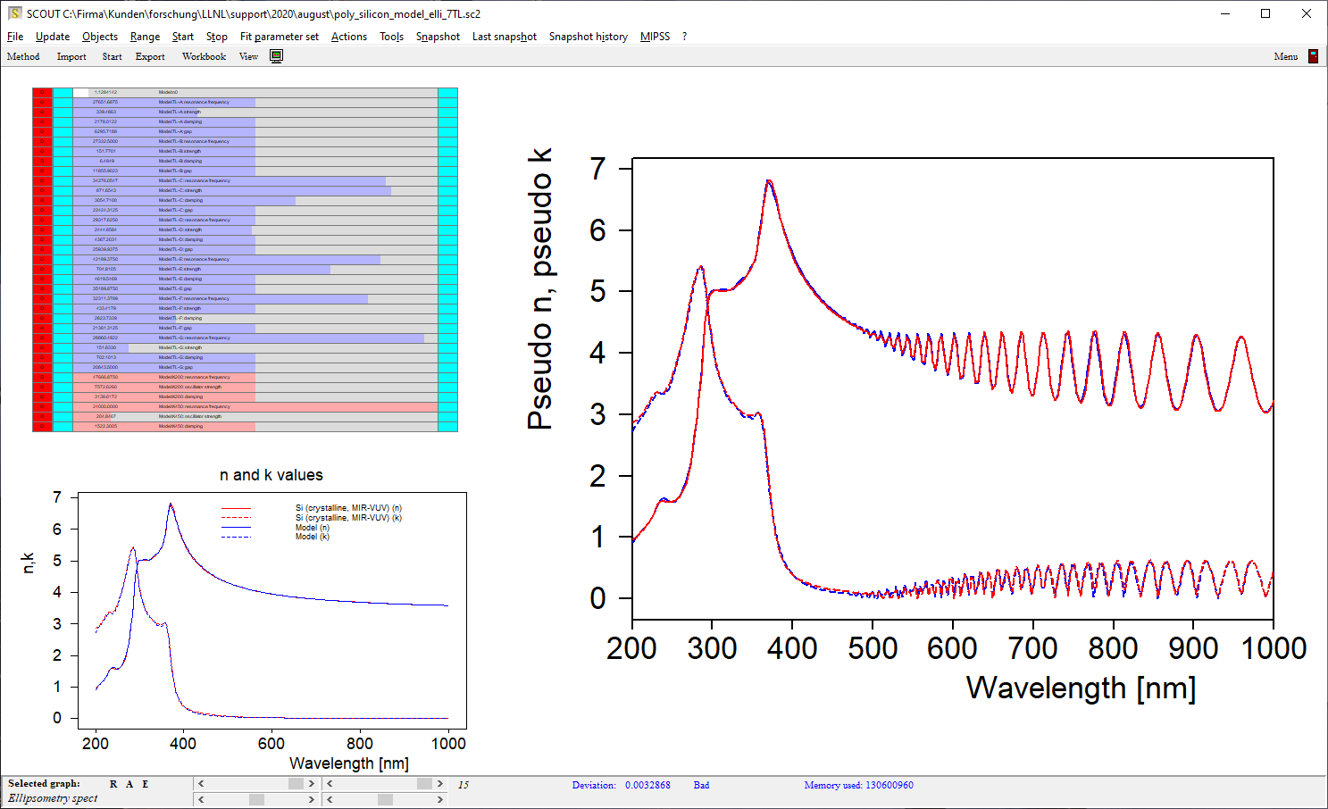
Depending on your patience (and the needs of the final application) you can add more features as you like, approaching the former table values of n and k more and more. I stopped my example at this level:
The model developed for silicon this way can now be saved to the optical constant database for future use. You can use it for studies of systematic variations of deposition conditions and generate tables like ‘resonance frequency vs deposition temperature’.
You can follow the strategy shown in this tutorial for all kinds of materials, as long as you get good tabulated values of n and k to start with.

