Tag Archives: SPRAY

New wafer object


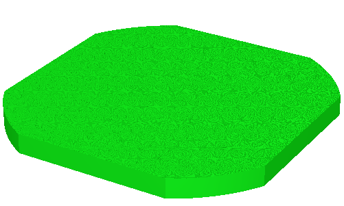
With SPRAY version 2.53 we have introduced a new geometric object called ‘wafer’ which represents a silicon wafer to be used in a solar cell. The wafer has a cylindrical base shape and is cut at the sides:

wafer

The bottom surface is textured with shapes that have been available in previous versions of SPRAY already.

The top surface can be textured the same way or using a new mechanism: In order to approach realistic textures you can now superimpose two textures which may have different shapes and periodicities. This opens a large variety of surface patterns (see examples below).

“Uniform” pyramids

A surface texture of regular pyramids of one and the same size looks like this (for an inclination angle of 54°):

wafer_pyramids_54

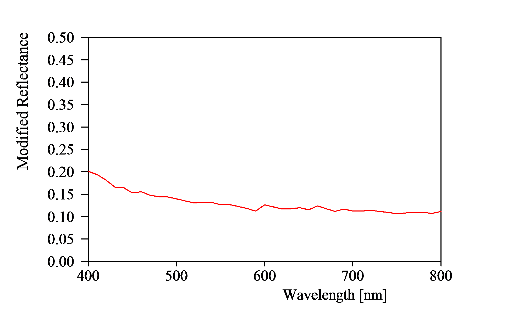
The reflectance spectrum in the spectral range 400 … 800 nm is this:

wafer_pyramids_54_spectrum

Average reflectance is 13.8%.

“Non-uniform” pyramids

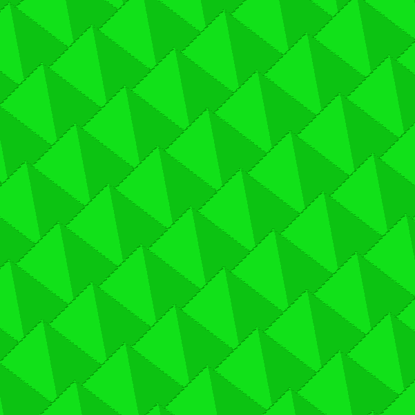
Big and small pyramids (with different heights and periodicities) mixed together:

wafer_pyramids_small_large


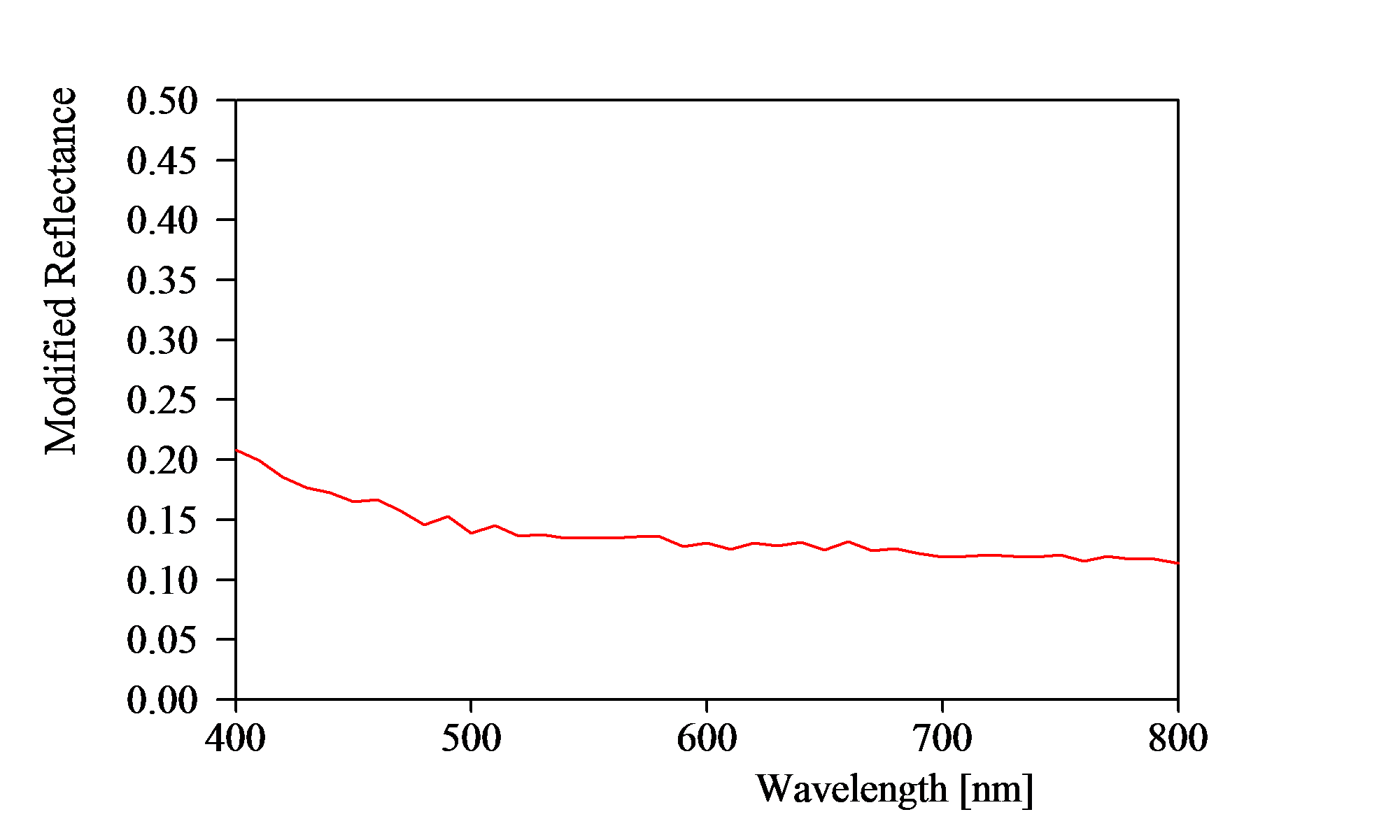
Reflectance of this texture:

wafer_pyramids_small_large_spectrum

Average in the range 400 … 800 nm: 13.2%

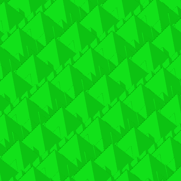
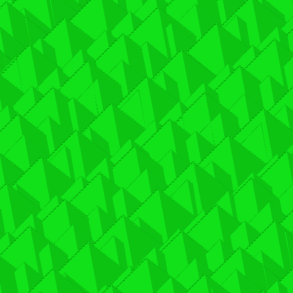
Big and medium sized pyramids mixed together – this looks quite realistic:

wafer_pyramids_medium_large


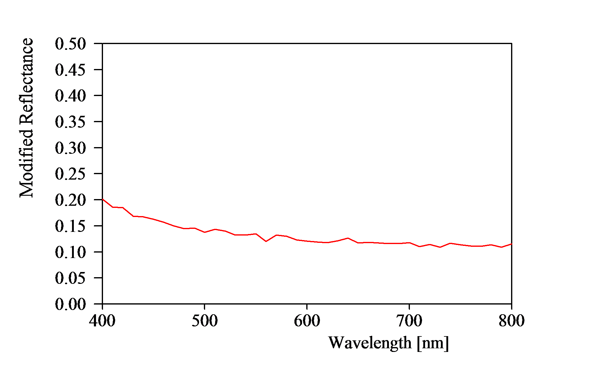
The reflectance of this kind of texture is this:

wafer_pyramids_medium_large_spectrum

Average reflectance: 13.0%

You may assign different layer stacks to the bottom, side and top surfaces of the wafer object. This way you can introduce AR coatings on top which are not deposited at the sides and below.

SPRAY surface textures

SPRAY is a powerful tool to optimize the performance of solar cells. In order to simplify the modeling of crystaline silicon PV modules we have added an easy way to define macroscopic surface texture. This new feature can be used for both the covering glass and the Si wafer surface.

A PV module consists of a silicon wafer with top and backside contacts:

wafer spray

The wafer is embedded in EVA:

wafer spray packed

The EVA is covered by glass which gives mechanical strength and protection for the next 30 years. In order to maximize the generation of electric power one may introduce an

  • anti-reflection (AR) layer between silicon and EVA
  • AR layer between glass and air
  • surface texture of the silicon wafer
  • surface texture of the cover glass
  • diffusely reflecting white backside
  • low-absorptive cover glass

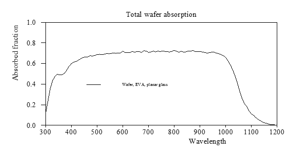
In order to find out how much the PV output is increased by these improvements one can perform realistic ray-tracing computations with SPRAY. This can save a lot of experimental work and costs. SPRAY performs 3D spectral ray-tracing and records where how much radiation is absorbed. It can, for example, output the spectrum of absorbed light in the wafer

wafer spray result1


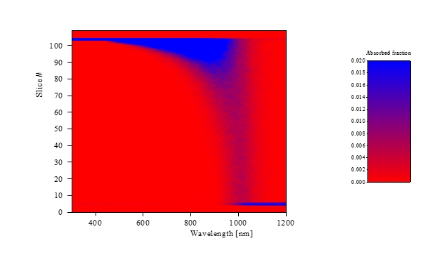
as well as the spatial distribution of absorbed light:

wafer spray absorption depth profile

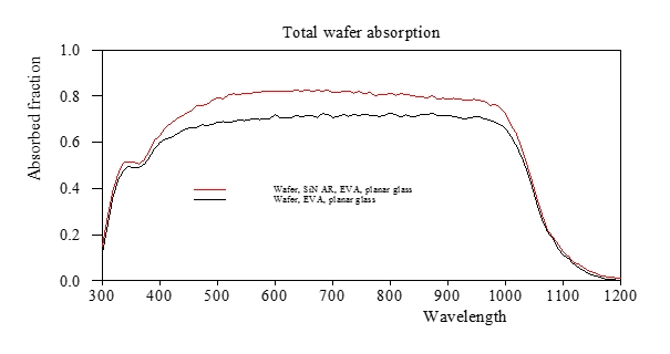
The graph below shows a comparison of the absorbed fraction with and without a simple AR coating (a single SiN layer) between silicon and EVA:

wafer spray simple SiN AR


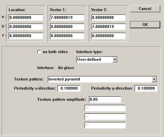
The modeling of macroscopic surface textures is now much easier using the new object type ‘Periodic surface texture’. This is a rectangle with a regular surface pattern in the x- and y-direction. You can set the periodicities in both directions and select a pattern type. Depending on the type of texture you can set additional parameters in the object dialog:

clip0001


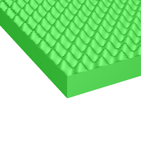
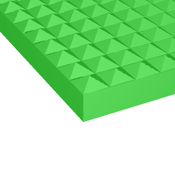
The available textures are the following:

Sine profile

clip0002


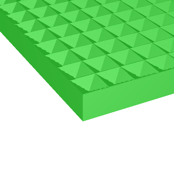
Pyramids
clip0003
Inverted pyramids
clip0004
Cones
clip0005
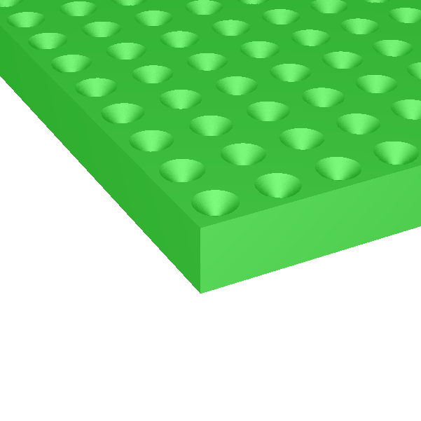
Inverted cones
clip0006
 
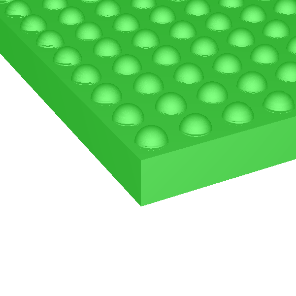
Half spheres
clip0007
 
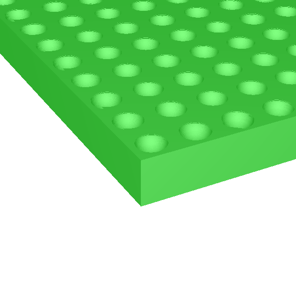
Inverted half spheres
clip0008