Besides optical spectra CODE computes sheet resistance values of layers stacks. A sheet resistance object in the list of integral quantities computes the current value and – with the ‘Optimize’ option turned on – the squared difference to a given target value.
If you type in a measured sheet resistance value as target value CODE optimizes a layer stack to reproduce measured electrical performance (only if the option ‘Optimize’ is switched on, of course). If you check the option ‘Combine fit deviation of integral quantities and spectra’ (File/Options/Fit) you can fit spectra and sheet resistance at the same time, balancing importance by setting proper weights for each quantity.
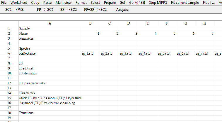
We have now added the ability to take into account measured sheet resistance values to batch fitting. In order to use this new feature you have to define a sheet resistance object in the list of integral quantities and name it ‘sheet resistance fit’. Set its ‘Optimize’ option ‘On’. Then generate a new batch fit based on the current model – or use an existing one. Here is an example of the results page:
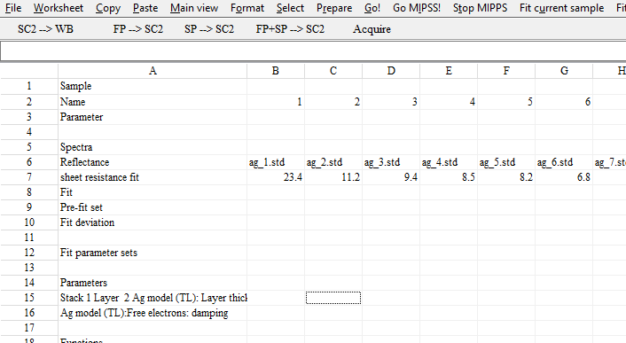
Note the empty line between the last spectrum (‘Reflectance’ in this case) and the line called ‘Fit’. Enter the key phrase ‘sheet resistance fit’ into the first column and type in or copy the measured values for each sample (i.e. for each column). The table should look like this now:
That’s all – you are now ready to start batch fitting. For each sample the measured values will be entered as target values and CODE will optimize both spectra and sheet resistance values.
You might encounter the difficulty that measured and simulated sheet resistance values do not easily agree. In this case you should check if your sample might show a depth gradient of the conductivity. A reason could be a depth dependent density of defects like grain boundaries within the layer. In such a case you should consider dividing the conductive layer into several parts with different damping constants of the charge carriers. You can read a discussion for silver and other conductive layers here.


